Rtl schematic Rtl schematic for the encoder circuit A). rtl schematic of proposed design 2 and proposed design 2
The Ultimate Guide to RTL Design - HardwareBee
Rtl schematic design of jpeg compression steps. Rtl schematic in detail of design Rtl design
The ultimate guide to rtl design
Rtl diagramRtl diagram of the proposed serial design 。 Rtl proposedXilinx running procedure with synthesis report rtl schematic, technlogy.
The rtl schematic for the modules the above figure represents the rtlDiseño rtl (nivel de transferencia de registros) frente a diseño de Rtl design and integration servicesRtl verilog.

Rtl schematic diagram
3: example of rtl design flowXilinx rtl schematic synthesis Rtl guide fpga asic tool ultimate layout needsRtl schematic design 1 generated by xilinx simulation.
Rtl-design for beginnersSchematic design A: rtl schematic for the proposed system designed.Rtl schematic of design process flow (screenshot)..

Schematic rtl figure3
Rtl design company chennaiB: internal design of rtl schematic. Schematic sdr rtl block diagram rtlsdr overallRtl githubusercontent methodology.
Rtl schematic diagram for design 1 by vcs9: rtl schematic of the implementation the layout of the design was Figure3 shows the rtl schematic of the design[rtl-sdr] rtl-sdr schematic.

Electrical – discrepancy between rtl schematic and behavioral
Rtl schematic of top module of the proposed designThe ultimate guide to rtl design Internal rtl schematic of proposed workRtl schematic report..
Rtl schematic design 2 generated by xilinx simulation after the rtlDigital circuits and systems Schematic diagram of model-based rtl design.
![[RTL-SDR] RTL-SDR Schematic - Programmer Sought](https://i2.wp.com/www.programmersought.com/images/833/3b834c92764c54eb0276d54aaf553689.png)

RTL schematic design 2 generated by Xilinx simulation After the RTL

RTL Verilog - javatpoint

RTL Schematic for the Encoder Circuit | Download Scientific Diagram

RTL schematic of design process flow (screenshot). | Download

The RTL Schematic for the modules The above figure represents the RTL
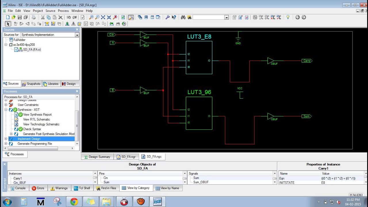
Xilinx Running Procedure with Synthesis Report RTL Schematic, Technlogy

RTL Design Company Chennai | RTL Design Services

The Ultimate Guide to RTL Design - HardwareBee